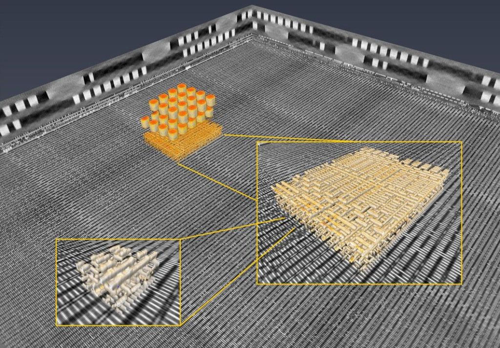
以灰度显示芯片的 3D 虚拟切片表示的艺术图像。图片:PSI
Researchers from the University of Southern California, as well as the Swiss Federal Institutes of Technology and the Paul Scherrer Institute (PSI) in Switzerland have invented a new non-destructive technique to reverse engineer an entire chip without damaging it. The technique is called ptychographic X-ray laminography and is actually an upgrade to a technique called ptychographic computed tomography that the researchers first announced in 2017.
来自南加州大学、瑞士联邦理工学院和瑞士 Paul Scherrer 研究所 (PSI) 的研究人员发明了一种新的非破坏性技术,可以对整个芯片进行逆向工程而不损坏它。该技术被称为叠层 X 射线层析成像,实际上是研究人员于 2017 年首次宣布的叠层计算机断层扫描技术的升级版。
What Is Ptychographic X-ray Laminography?
什么是叠层 X 射线断层扫描?
According to the researchers, the ptychographic X-ray laminography is the only non-destructive technique that doesn’t require cutting up the chip. The technology allows for the imaging of the entire chip and to zoom into specific areas.
研究人员表示,叠层X射线层析成像是唯一不需要切割芯片的非破坏性技术。该技术可以对整个芯片进行成像并放大特定区域。
In comparison, existing reverse engineering technologies require taking a chip apart layer by layer and mapping them using different imaging techniques such as optical microscopy for the larger elements to electron microscopy for the smallest ones.
相比之下,现有的逆向工程技术需要将芯片逐层拆开,并使用不同的成像技术对它们进行映射,例如针对较大元件的光学显微镜到针对最小元件的电子显微镜。
Talking about the ptychographic X-ray laminography technology, professor of electrical and computer engineering at University of Southern California Anthony F. J. Levi, told IEEE Spectrum that:
南加州大学电气与计算机工程系教授 Anthony F. J. Levi 在谈到叠层 X 射线层析技术时,对 IEEE Spectrum 表示:
“It’s the only approach to non-destructive reverse engineering of electronic chips—[and] not just reverse engineering but assurance that chips are manufactured according to design. You can identify the foundry, aspects of the design, who did the design. It’s like a fingerprint.”
“这是对电子芯片进行非破坏性逆向工程的唯一方法,不仅是逆向工程,而且还保证芯片是根据设计制造的。您可以识别代工厂、设计的各个方面以及设计者。就像指纹一样。”

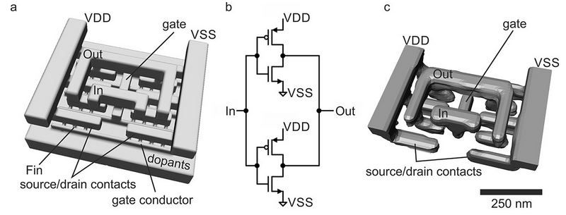
叠层X射线层析成像可以揭示逆变器的金属部件[右]。显示出与电路的良好匹配[中,左]。图片:PSI
The researchers’ prior technique had to use too many x-rays, which wouldn’t result in a very clear image of the chip. The new technique can shoot the x-rays at an angle (61 degrees to be exact) but still loses some chip information.
研究人员之前的技术必须使用太多的 X 射线,这不会产生非常清晰的芯片图像。新技术可以以一定角度(准确地说是 61 度)发射 X 射线,但仍然会丢失一些芯片信息。
However, these gaps can be filled by knowing what type of interconnects are supposed to be in those specific locations. Knowing the design rules of the chip before starting the process can allow for the use of even fewer photons, so the final image should be even more clear with less information loss.
然而,可以通过了解这些特定位置中应该有什么类型的互连来填补这些空白。在开始流程之前了解芯片的设计规则可以允许使用更少的光子,因此最终图像应该更加清晰,信息损失也更少。
What Are the Implications For This New Technology?
这项新技术有何影响?
The technology could have all sorts of implications, such as allowing integrated circuit designers to verify if a chip matches its promised specifications.
该技术可能具有各种影响,例如允许集成电路设计人员验证芯片是否符合其承诺的规格。
Another benefit could be that having a cheaper way to reverse engineer chips would allow new entrants in the chip market to study the incumbents’ designs and then compete more effectively in the market. Reverse engineering is generally not illegal, but the new technology may not exactly make the chip incumbents happy that it exists.
另一个好处可能是,采用更便宜的方法对芯片进行逆向工程将使芯片市场的新进入者能够研究现有企业的设计,然后更有效地在市场上竞争。逆向工程通常并不违法,但新技术可能并不会让芯片厂商对其存在感到高兴。
Furthermore, easier and cheaper ways to reverse engineer chips would also allow for the finding of more security flaws in hardware. Intel may not be able to catch a break anytime soon, even with the new hardware mitigations it’s researching.
此外,更简单、更便宜的芯片逆向工程方法也将有助于发现更多硬件安全漏洞。即使英特尔正在研究新的硬件缓解措施,它也可能无法很快休息。
Using such technology, governments that don’t trust chipmakers from other countries could also more easily discover if a chip has a hidden backdoor in it, or not. There was recently a large controversy started by a Bloomberg report about a possible backdoor in Supermicro’s motherboards.
使用这种技术,不信任其他国家芯片制造商的政府也可以更容易地发现芯片中是否存在隐藏的后门。最近,彭博社的一篇关于 Supermicro 主板可能存在后门的报道引发了一场大争议。
The story was controversial because many experts wanted to see more evidence that what Bloomberg was reporting was real. If a non-destructive reverse engineering technology would have been available and easily accessible by many of the chipmakers’ own customers or even security researchers, it would have been easier to get to the bottom of the story and find out if the allegation was true or not.
这个故事引起了争议,因为许多专家希望看到更多证据证明彭博社报道的内容是真实的。如果非破坏性逆向工程技术能够被许多芯片制造商自己的客户甚至安全研究人员轻松使用,那么就可以更容易地了解故事的真相并查明指控是否属实或不是。

